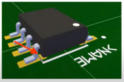
I have a question about routing style of pads with the same functionality belonging to one chip. I draw a picture in Paint (fictional IC; let it be the SOIC8 footprint). GND is only as example (it
What is a Pad in PCB Design and Development
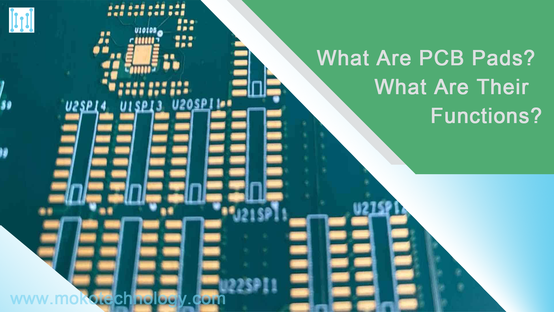
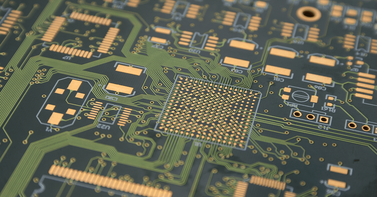
What Are PCB Pads? What Are Their Functions?
What Role Does PCB Copper Balance Play in PCB Fabrication?
Working with Pads & Vias in Altium Designer Altium Designer 24 Technical Documentation

Via-in-Pad - PCB Prototype the Easy Way - PCBWay
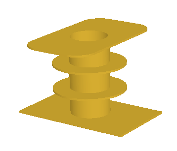
Pad Stacks, Advanced PCB Design Blog
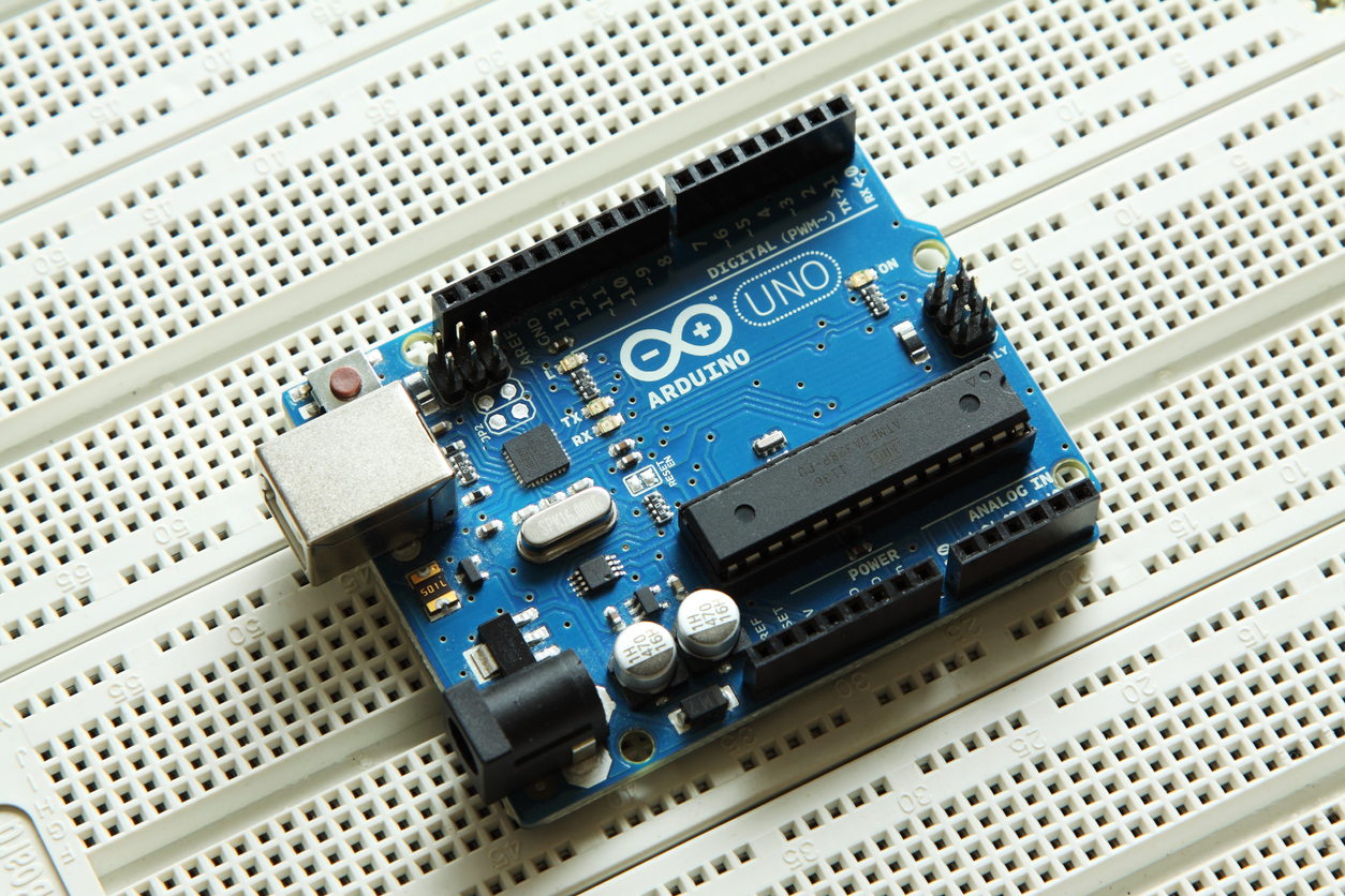
A Guide to Arduino PCB - KnowHow

Types of PCB Pads PCB Knowledge - PCB Basic Information - PCBway
soldering - How do I connect components when using a circuit board with pads but no traces? - Electrical Engineering Stack Exchange
How to Design Correct PCB Footprints
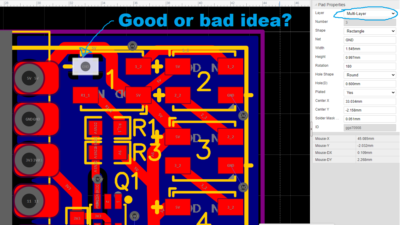
PCB Design, good or bad idea to use multilayer GND pads (to stitch plane and connect LED)? - Random or Off Topic - V1 Engineering Forum